Anodizing Aluminum Defects
Basic Concepts of Anodizing Treatment
- Principle: An oxide film is formed on the surface of metals (mainly aluminum alloys) through electrochemical methods, which is a key technology in metal surface treatment.
- Core Purpose: To enhance the corrosion resistance, wear resistance and insulation of aluminum alloy, while improving the appearance and durability of anodized aluminum.
General Classification of Aluminum Alloy Anodizing Defects
Based on "nature and impact", aluminum alloy anodizing defects are divided into three categories. Among them, surface defects account for the highest proportion and have the highest rejection rate, appearance and performance defects are prone to causing batch rejection, form and dimensional defects are relatively rare. The specific classification is as follows:
Surface Defects
- Characteristics: Most common in production sites, directly affecting appearance and basic performance.
- Main Defect Types: Spotted defects, uneven appearance defects, and other specific surface defects (such as scratches, Adhesion (anodizing/electrophoresis), etc.).
Appearance and Performance Defects
- Characteristics: Related to functional indicators, prone to batch rejection.
- Main Defect Types: Sealing failure, oxide film thickness non-compliance, non-compliance of paint film hardness/corrosion resistance.
Form and Dimensional Defects
- Characteristics: Low proportion, mostly originating from previous processes.
- Main Defect Types: Holding device impression exceeding standard, lack of wall thickness after rework.
Details of Each Type of Defect
Surface Defects: The Core Category
Defect Name: Fingerprint-like corrosion
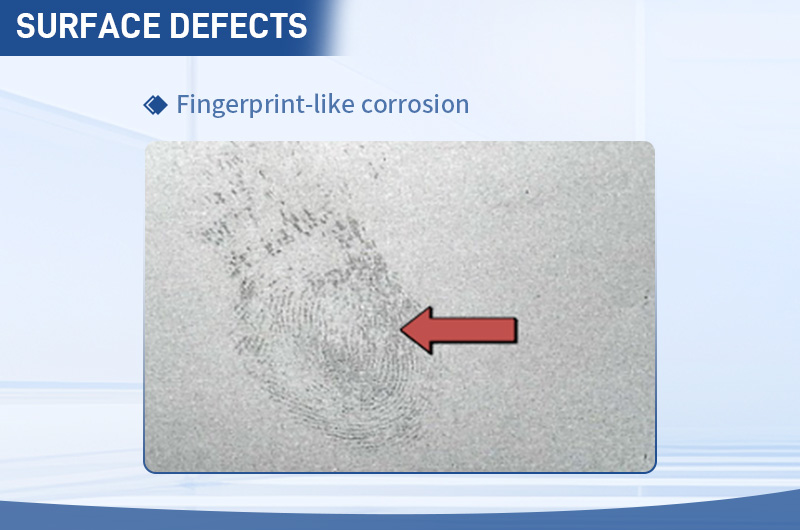
Definition: Fingerprint or glove-like corrosion spots.
Characteristics: Caused by contact with human sweat (sodium chloride, lactic acid), mostly in the form of fingerprint-like pitting corrosion.
Causes:
- Dirty gloves during extrusion/racking.
- Storage for more than 6 hours after racking.
- Incomplete degreasing before anodizing.
Solutions:
- Timely replacement of dirty/wet gloves.
- Anodizing within ≤6 hours after racking.
- Extending degreasing time.
Defect Name: Scratch
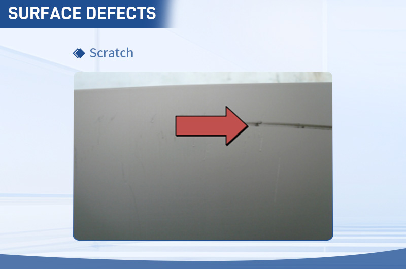
Definition: Damaged scratches on the surface of profiles.
Characteristics: Thin hairline/point-like scratches with glinting luster, including handling/transportation scratches.
Causes:
- Collision between profiles, or between profiles and frames.
- Improper packaging or rough operation.
Solutions:
- Handle with care and prohibit collision.
- Cover the edges of material frames with protective rubber sleeves.
- Hoist ≤6 rows of materials and place profiles of different lengths separately.
- Use intact padding strips.
Defect Name: Adhesion (anodizing/electrophoresis)
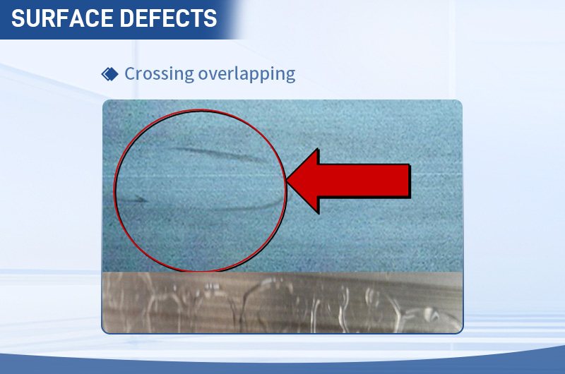
Definition: Abnormal film formation due to overlapping of materials during anodizing/electrophoresis.
Characteristics: Film-free or thinned film areas with overlapping marks, occasionally showing iridescent interference colors.
Causes:
- Too dense racking spacing.
- Insufficient racking tension, leading to profile sliding and overlapping during water washing.
Solutions:
- Use 3 aluminum wires for racking electrophoretic materials (2 for small materials) with a spacing of 2-3 fingers.
- Racking the sagging profiles with a middle wire.
- Increase the lowering angle and slow down the exhaust..
Defect Name: Rough etching
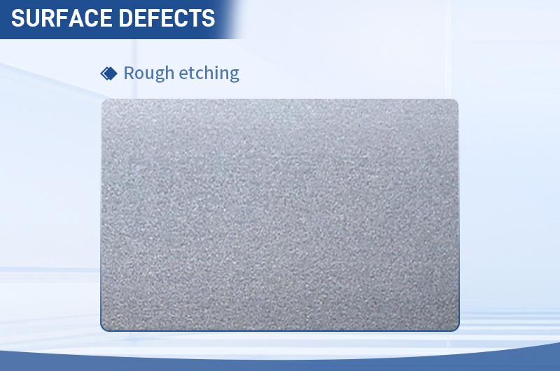
Definition: Surface roughness caused by excessive alkaline etching of aluminum materials.
Characteristics: Dull and rough surface, affecting dimensional accuracy in severe cases.
Causes:
- Excessively high temperature/concentration of the alkaline bath.
- Too low aluminum ion content in the alkaline bath.
- Long etching time, bath contamination, or frequent rework.
Solutions:
- Adjust alkaline bath parameters (concentration, aluminum ion content, temperature).
- Control alkaline etching time.
- Regularly clean bath dregs and reduce rework.
Defect Name: Insufficient etching
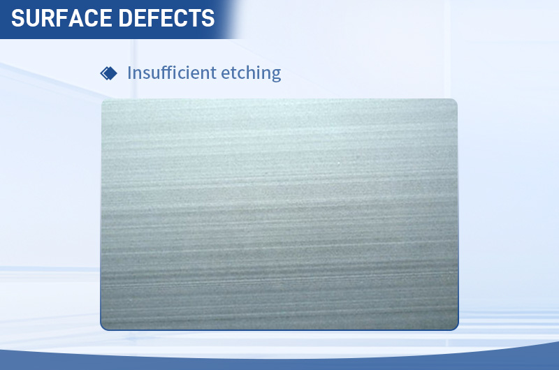
Definition: Incomplete alkaline etching, failing to eliminate surface defects.
Characteristics: No matte surface effect or failure to meet customer requirements.
Causes:
- Too low temperature/concentration of the alkaline bath.
- Short alkaline etching time.
- Too high aluminum ion content in the alkaline bath.
Solutions:
- Control the temperature/concentration of the alkaline bath.
- Extend alkaline etching time.
- Adjust aluminum ion concentration.
Defect Name: Uneven degreasing
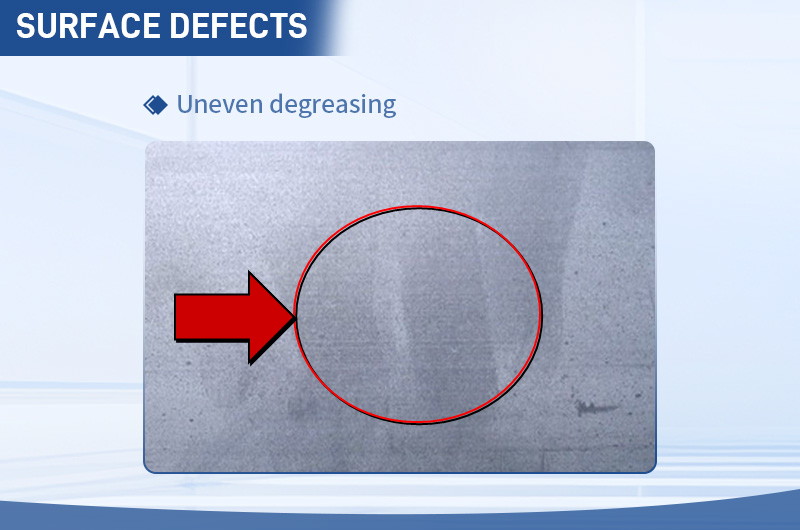
Definition: Uneven alkaline etching caused by incomplete degreasing.
Characteristics: Uneven gloss after anodizing, and color spots/uneven color after coloring.
Causes:
- Insufficient degreasing time.
- Insufficient effective components in the degreasing bath.
- Severe oil contamination on the workpiece surface.
Solutions:
- Add degreasing agent.
- Soak for ≥3 minutes.
- Pre-treat heavily oil-contaminated workpieces with manual wiping.
Defect Name: Anodic oxide bubbles
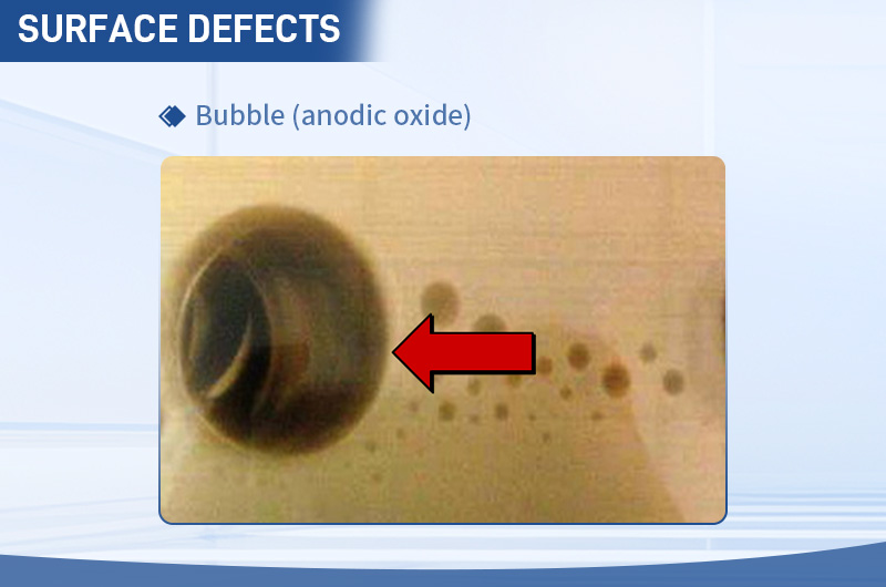
Definition: Local film-free or non-coloring areas caused by retention of electrolytic gas/stirring air.
Characteristics: Thin or no film at gaps/corners, and uneven color after coloring.
Causes:
- Improper hoisting angle.
- Fast tank entry speed;
- Profile shape unfavorable for exhaust.
- Damaged defoaming bags.
Solutions:
- Control the lowering angle.
- Extend pre-immersion time.
- Replace damaged defoaming bags.
Defect Name: Incomplete film removal
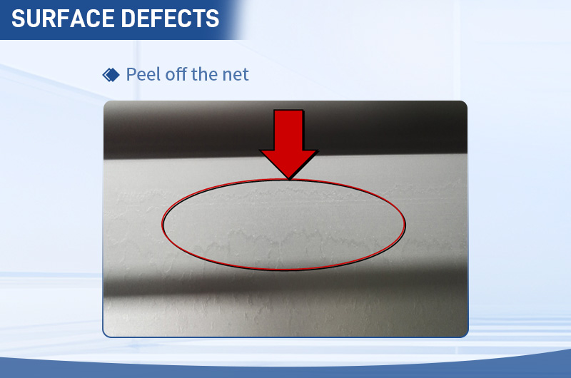
Definition: Incomplete removal of old oxide film from reworked profiles.
Characteristics: Uneven peeling layer after re-anodizing, failing to form a new film.
Causes:
- Insufficient soaking time in sulfuric acid.
- Insufficient alkaline etching time for film removal.
Solutions:
- Extend soaking time in sulfuric acid.
- Extend alkaline etching time.
Defect Name: Rinse water corrosion
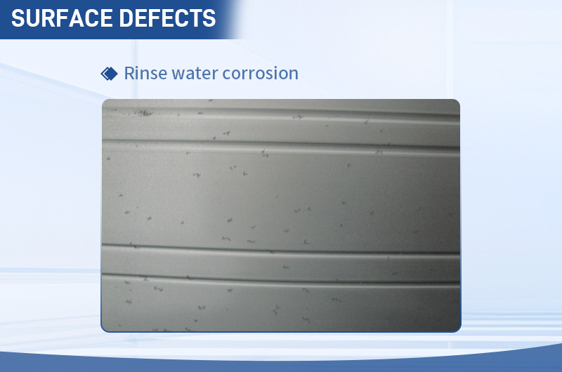
Definition: Spotted corrosion during water washing caused by material impurities.
Characteristics: Black dots at the center as cores, spreading outward in a snowflake/octopus claw shape.
Causes:
- Zinc/gallium in profiles reacting with Cl⁻/F⁻in the water washing bath.
- Long retention time in the water bath after neutralization.
- Water bath contamination.
Solutions:
- Control zinc/gallium content in aluminum rods.
- Retain in the water bath for ≤10 minutes.
- Maintain nitric acid concentration of 5%-8% in the neutralization bath.
- Increase drainage volume.
Defect Name: White spots (anodic oxide)
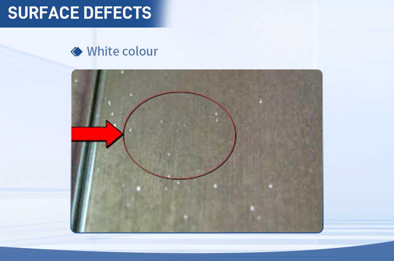
Definition: White dot-like uncolored marks on the surface without film peeling.
Characteristics: Cracks on the film, uncolored areas around the cracks, distributed along the extrusion direction, and detectable by touch.
Causes:
- Inclusions in the alloy.
- Alkali mist adhering to the oxide film.
Solutions:
- Strictly control the casting rod process.
- Anodize as soon as possible after racking.
- Improve workshop ventilation.
Defect Name: Electrical burning
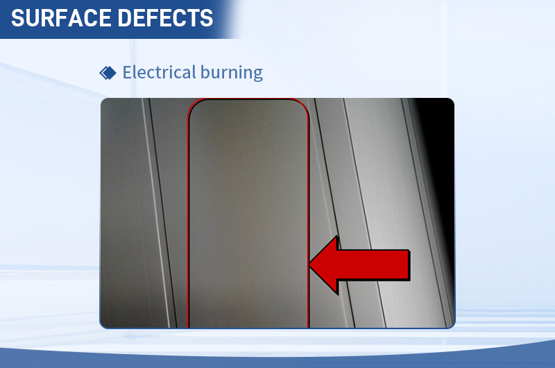
Definition: Burning/breakdown caused by excessive local current density during anodizing.
Characteristics: Black/yellow burning marks on the film, and profile breakdown in severe cases.
Causes:
- Excessive current density.
- Short circuit or poor contact between profiles and cathodes.
- Rapid current rise.
- Damaged cathodes or small cathode area.
Solutions:
- Control current density at 1.2-1.5mA/dm².
- Prohibit profiles from touching cathodes.
- Polish racking rods and tighten jigs.
- Standardize soft current rise.
- Replace cathode plates.
Defect Name: Non-metallic inclusions
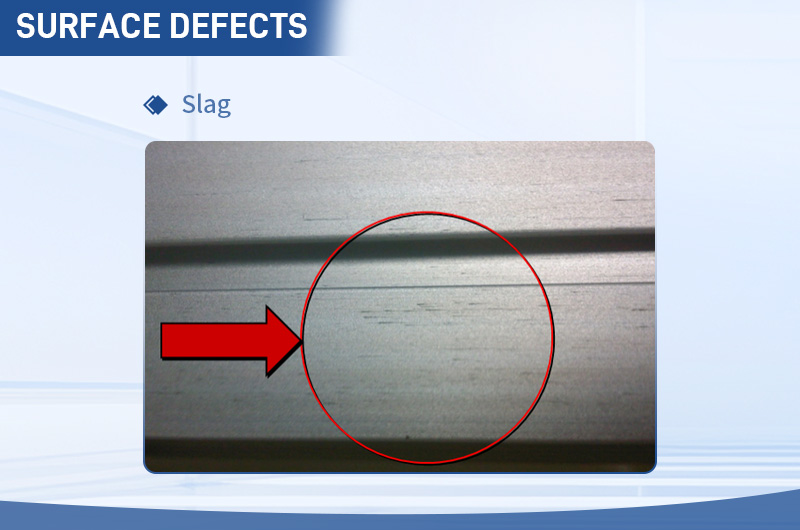
Definition: Non-metallic inclusions in the metal structure, exposed on the surface after anodizing.
Characteristics: Discontinuous line-shaped, consistent with the extrusion direction, invisible during extrusion but visible after anodizing.
Causes:
- Misalignment between the extrusion cylinder and rod, leading to foreign matter entrainment.
- Die orifices too close to the outer circle.
Solutions:
- Center the die orifices (reduce the circumcircle of the shunt hole for hollow profiles).
- Check extrusion alignment and maintain residual pressure.
- Remove foreign matter.
- Control the temperature of the extrusion pad and heat the cylinder/ingot.
Defect Name: Spalling
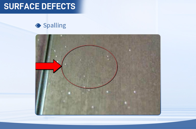
Definition: Spot-like peeling of the oxide film during coloring, leading to non-coloring.
Characteristics: Irregularly distributed white dots or blocks, undetectable by touch.
Causes:
- Excessive coloring voltage/time.
- Contamination of the coloring solution.
- Thin or uneven oxide barrier film.
Solutions:
- Correct coloring parameters.
- Remove impurities from the coloring solution.
- Increase anodizing voltage.
Defect Name: Black spots
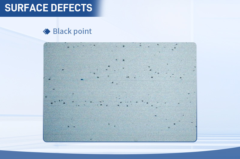
Definition: Black star-shaped corrosion pits on the aluminum surface.
Characteristics: Irregularly distributed black dots, with no oxide film at the corrosion points.
Causes: Excessively high chloride ion concentration in the anodizing electrolyte.
Solutions: Replace the bath solution and stabilize the anodizing bath parameters.
Defect Name: Film cracking (anodic oxide)
Definition: Film cracking caused by large difference in thermal expansion coefficient between the oxide film and the substrate, or external force/high temperature.
Characteristics: Flake-like scales visible when observed obliquely under strong light.
Causes:
- Excessively long sealing time.
- No air stirring for high-film-thickness materials, leading to no heat exchange.
- Rough operation during unracking.
Solutions:
- Adjust sealing time.
- Aerate and stir during anodizing of high-film-thickness materials.
- Standardize unracking operation.
Defect Name: Iridescence
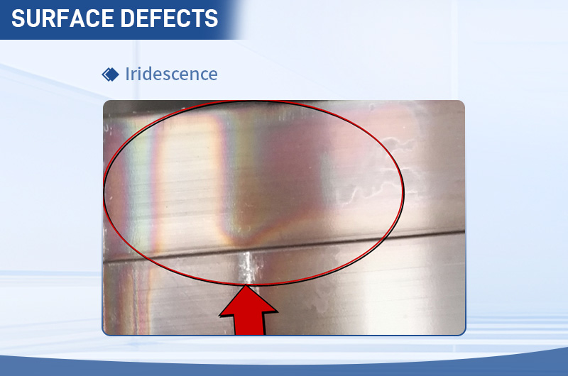
Definition: Optical interference phenomenon, with abnormal thin films (rainbow films/interference films) on the surface.
Characteristics: Rainbow colors visible when observed obliquely.
Causes:
- Silica/phosphate in the hot sealing bath.
- High concentration/temperature or long time of the cold sealing bath.
- Poor anodizing electrolysis.Corrosion of the sealing film.
Solutions:
- Adjust bath composition.
- Reduce bath temperature and shorten sealing time.
- Lower nickel ion content in the sealing bath.
- Clean bath dregs and filter the bath solution.
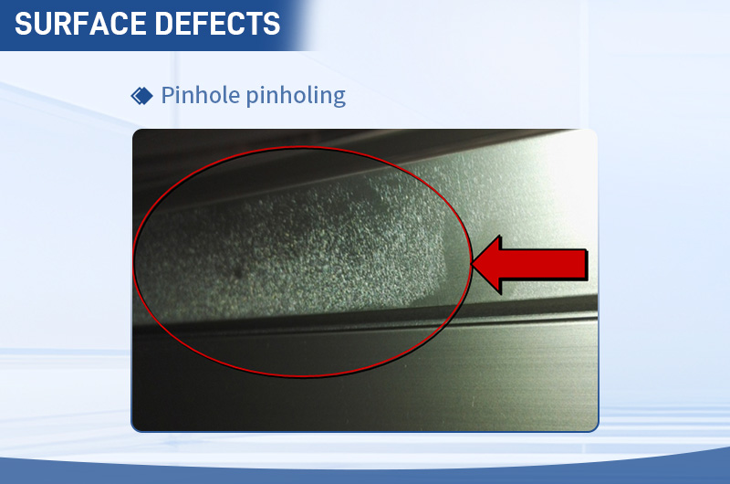
Defect Name: Pinhole (film)
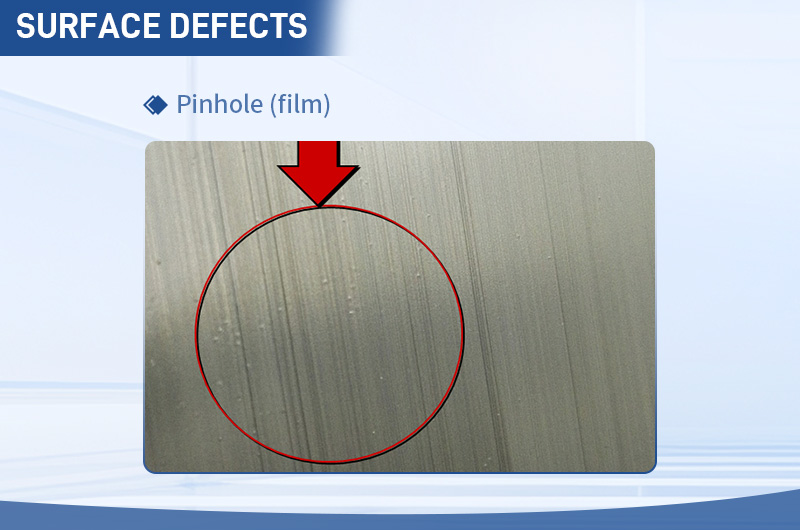
Definition: Pinhole-like pitting corrosion on the paint film surface.
Characteristics: Small hole-like depressions/penetrations, more visible when observed obliquely.
Causes:
- Air bubble entrainment when entering the electrophoresis bath;
- Air intake in the circulation system.
- Damaged defoaming bags or high voltage.
- Bath contamination, high temperature, or low pH.
- Incomplete oil removal in pre-treatment.
- Long storage of blanks.
Solutions:
- Increase the lowering angle and shake up and down.
- Replace defoaming bags/filter bags.
- Reduce voltage and control bath temperature.
- Adjust bath parameters.
- Strengthen oil removal and anodize in time.
Defect Name: Chromatic aberration
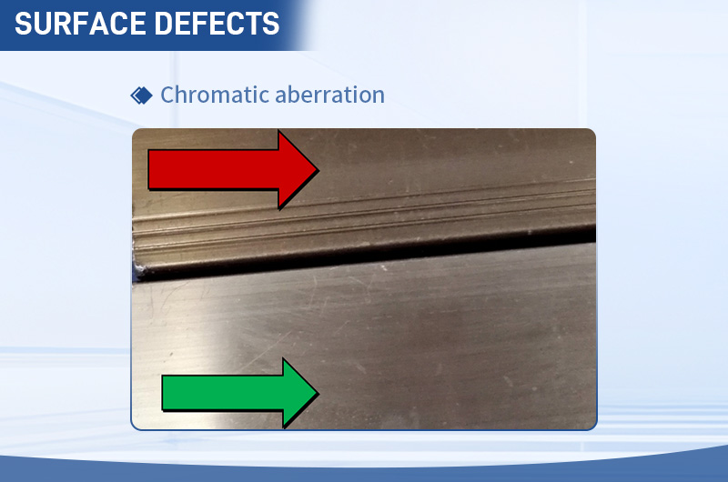
Definition: Visual color difference from the standard plate.
Characteristics: Color deviation from the standard plate after anodizing and coloring.
Causes:
- Poor conductivity.
- Loose profile clamping.
- Inaccurate color matching during coloring.
Solutions:
- Polish the conductive rod until the substrate color is exposed.
- Tighten the profiles.
- Match colors according to the standard plate and correct in time.
Defect Name: Acid/alkali water corrosion
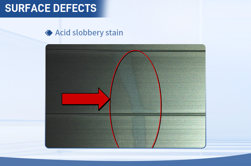
Definition: Corrosion of the profile surface by residual acid/alkali water.
Characteristics: White flow marks or round spots on the surface.
Causes:
- Residual acid/alkali solution on jigs/material racks.
- Incomplete cleaning of the profile surface.
- Crossing the material racks after sealing.
Solutions:
- Thoroughly clean jigs/material racks.
- Clean the small inner cavity of profiles multiple times.
- Do not cross the material racks.
- Rinse the conductive girders.
Defect Name: Sealing smut
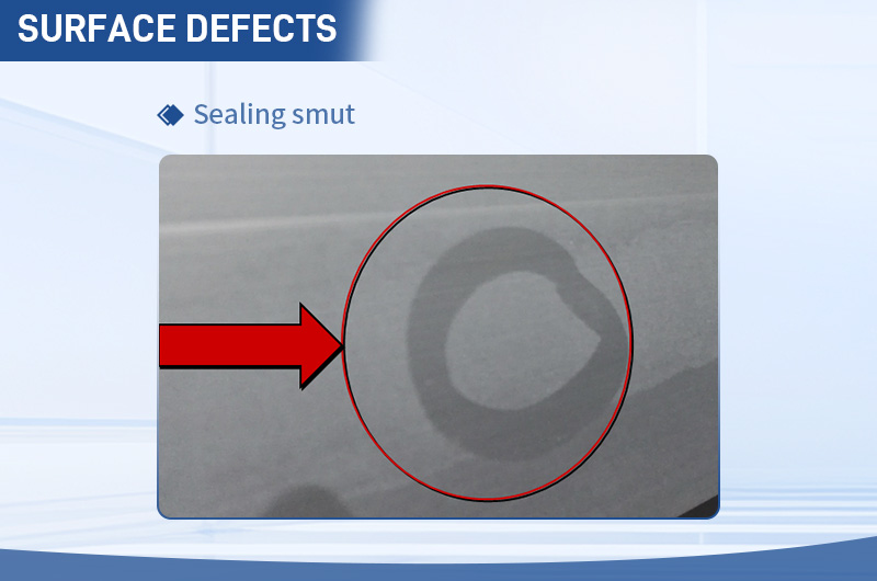
Definition: Calcium deposits adhering to the surface after sealing.
Characteristics: Wipeable white smut on anodized profiles, and hard-to-wipe yellow smut on colored profiles.
Causes:
- High calcium/magnesium ion content in the sealing bath.
- Uncleaned turbid substances in the bath.
- Long sealing time or aged bath solution.
Solutions:
- Ensure clean water in the water washing bath.
- Filter the sealing bath solution.
- Control sealing time.
- Replace with new bath solution.
Defect Name: Local absence of electrophoretic film
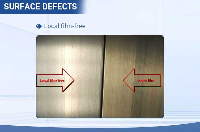
Definition: Failure to coat the organic paint film during electrophoresis.
Characteristics: Low surface gloss, rough and sticky to the touch.
Causes:
- Poor conductivity.
- Long water washing time in RO1/RO2.
- High solvent content in the water washing bath.
- High pH of the electrophoresis bath.
- High temperature or long soaking time in the hot water bath.
Solutions:
- Check the circuit/racking.
- Control water washing time to ≤2-3 minutes.
- Control solvent content.
- Detect and adjust pH.
- Control the process of the hot water bath.
Defect Name: Dust stain
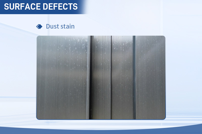
Definition: Small particles formed by dust and other foreign matter adhering to the surface or under the paint film.
Characteristics: Irregularly distributed dots, with a raised feel to the touch.
Causes:
- Dirty water washing bath or high conductivity before electrophoresis.
- Mechanical impurities in the electrophoresis bath.
- Dust in the workshop/curing oven.
Solutions:
- Replace water in the water washing bath and test regularly.
- Strengthen the filtration of the electrophoresis bath.
- Use independent ventilation and clean regularly.
- Clean the curing oven and replace the filter screen.
Defect Name: Bubbles (electrophoretic film)
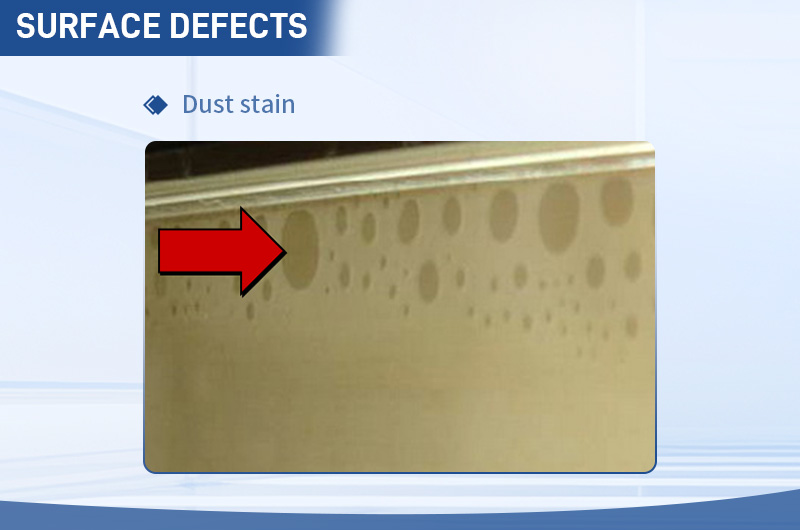
Definition: Bubble marks formed by bubbles adhering to the profile surface.
Characteristics: Irregular round bubble marks of varying sizes.
Causes:
- Air bubble entrainment when entering the electrophoresis bath.
- Micro-bubbles in the paint solution.
- Insufficient entry angle.
- Unclosed valves leading to air intake.
- Low solvent A content.
Solutions:
- Increase the lowering angle and stand for 30 seconds before energizing.
- Check defoaming bags.
- Add solvent B or increase circulation.
- Tighten valves.
- Supplement solvent A.
Defect Name: Powdering (JIS)
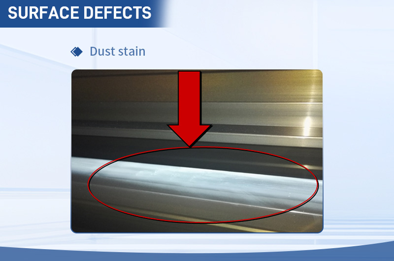
Definition: White powder formed on the film surface after anodizing.
Characteristics: White powdery and opaque film, easy to fall off when wiped by hand.
Causes:
- High electrolyte temperature, aluminum ion content, or current density.
- Long anodizing/immersion time.
- Inadequate bath stirring.
- Dense racking.
Solutions:
- Adjust electrolyte temperature.
- Separate excess aluminum ions.
- Control current, anodizing, and immersion time.
- Aerate and stir.
- Control racking spacing.
Defect Name: Yellowing(combined anodic oxide film)
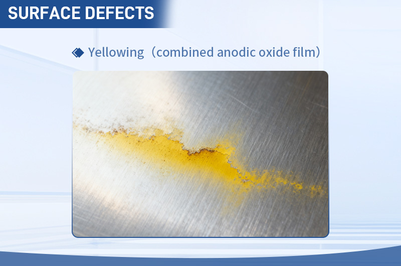
Definition: Yellowing of the paint film or oxide film.
Characteristics: Overall yellowing of the composite film on the profile.
Causes:
- Too thick coating.
- High curing temperature or long curing time.
- Contaminated electrophoresis bath or poor paint quality.
- Long soaking in water after anodizing.
Solutions:
- Reduce coating thickness.
- Adjust oven temperature to the process range.
- Refine the bath solution and select stable electrophoretic paint.
- Control the quality and time of water washing.
Defect Name: Gel adhesion (electrophoretic)
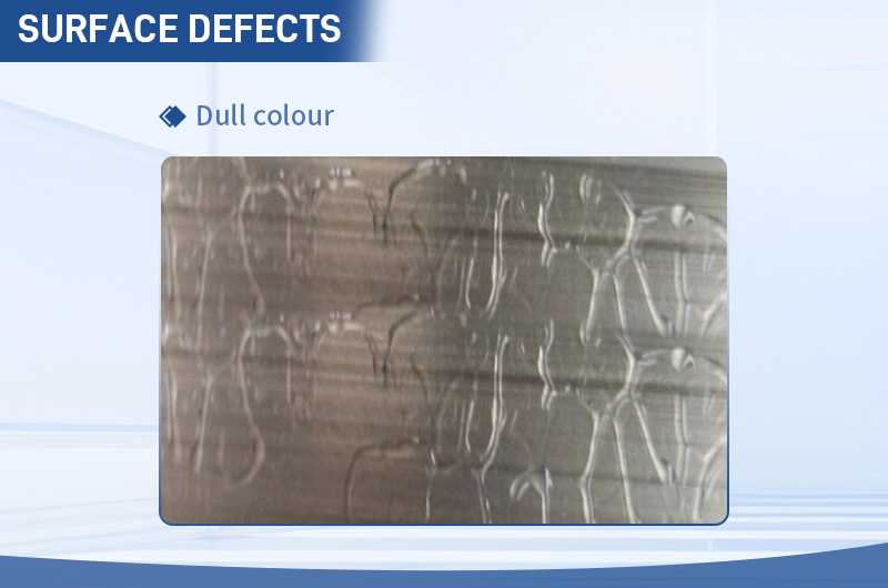
Definition: Granular electrophoretic paint adhering to the surface after electrophoresis curing.
Characteristics: Irregularly distributed particles of varying sizes.
Causes:
- Old paint adhering to the walls of the electrophoresis bath/RO water washing bath.
- Acid entrainment in the bath leading to resin agglomeration.
- Uneven stirring after adding paint.
Solutions:
- Regularly clean the bath body.
- Prevent acid entrainment.
- Stir for ≥30 minutes after adding paint before pumping into the main bath.
Defect Name: Paint streaks/residue (electrophoretic)
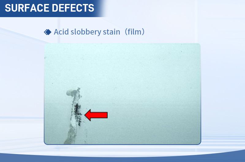
Definition: Paint spots or paint flow marks on the surface after electrophoresis curing.
Characteristics: Irregular paint spots/flow marks on the paint film surface.
Causes:
- Long retention time after exiting the electrophoresis bath.
- Improper paint concentration.
- Incomplete water washing.
- High solid content in the RO2 bath.
- Acid/alkali water dripping from the conductive girder.
Solutions:
- Retain for ≤1 minute after exiting the bath.
- Control paint concentration.
- Extend water washing.
- Reduce solid content in the RO2 bath.
- Spray and clean the girder.
Defect Name: Water spot
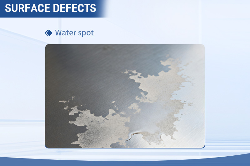
Definition: Spots or water drop-like patterns (watermarks) formed by water droplets adhering to the paint film surface before/during curing.
Characteristics: Prone to occur on horizontal/oblique parts, with irregular dot/drop-like patterns.
Causes:
- Water droplets adhering to the semi-dry paint film;
- Impurities in water droplets.
- Poor quality or short time of hot pure water washing.
Solutions:
- Extend water draining time.
- Ensure the quality and soaking time of the hot water bath.
Defect Name: Bubbles (coloring process)
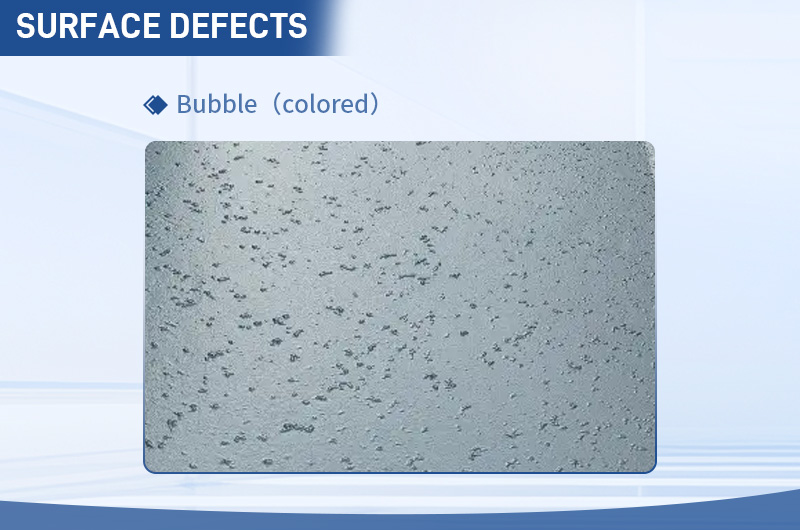
Definition: Bubble-like color spots formed by gas retention hindering the entry of coloring ions into the film pores during electrolytic coloring.
Characteristics: Thin or no film at gaps/corners, with uneven coloring.
Causes:
- Improper hoisting angle.
- Fast tank entry speed.
- Profile shape unfavorable for exhaust.
- Damaged defoaming bags.
Solutions:
- Control the lowering angle.
- Extend pre-immersion time.
- Replace damaged defoaming bags.
Appearance and Performance Defects: 4 Types, Related to Core Functional Indicators
Defect Name: Sealing failure
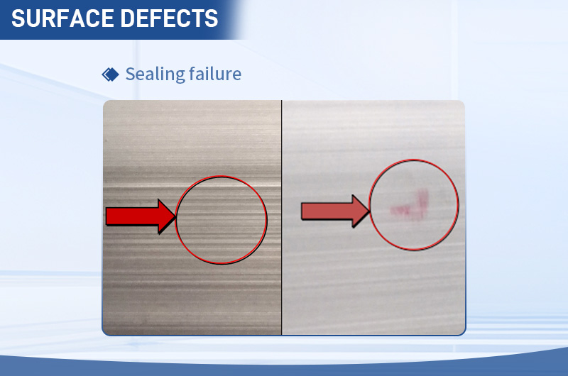
Causes:
- The sealing process is short and the temperature is low.
- Abnormal bath pH.
- Excessive film thickness.
Solutions:
- Extend sealing time.
- Adjust temperature/pH.
- Determine sealing time based on film thickness.
Defect Name: Oxide film thickness non-compliance
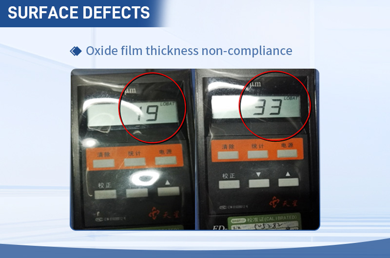
Causes:
- Miscalculation of anodizing time.
- Inaccurate current of the silicon machine.
- Loose racking.
Solutions:
- Calculate time according to the formula.
- Check current output.
- Tighten racking.
Defect Name: Pencil hardness non-compliance
Causes:
- Low hot water temperature.
- Insufficient curing temperature/time.
- Aged bath solution.
Solutions:
- Control hot water temperature.
- Adjust curing parameters.
- Replace part of the bath solution.
Defect Name: Corrosion resistance non-compliance
Causes:
- Thin paint film.
- Contamination of the hot water/pure water bath.
- High acid value of the bath solution.
Solutions:
- Ensure paint film thickness.
- Replace filter bags.
- Adjust acid value (refined C tower).
Form and Dimensional Defects: 2 Types, Low Proportion
Defect Name: Wire binding impression excess
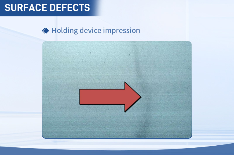
Causes:
- Poor positioning of conductive rods.
- Loose racking.
- Lowering angle < 30°.
Solutions:
- Position conductive rods;
- Tighten racking.
- Ensure lowering angle > 30°.
- Use compliant conductive rods.
Defect Name: Reduced wall thickness due to rework
Causes:
- Poor dimensional accuracy of extruded incoming materials.
- Frequent anodizing rework.
Solutions:
- Inspect incoming materials before racking.
- Ensure one-time qualification as much as possible.
Summary of Defect Causes
- Out-of-control process parameters: Abnormal bath solution (e.g., sulfuric acid concentration, Cl⁻>200ppm, aluminum ions>20g/L, pH, temperature), improper electrical parameters (e.g., current density, voltage, time).
- Equipment and tooling issues: Failures of jigs/conductive rods/defoaming bags, failure of stirring/filtration/insulation, inaccurate current of the silicon machine.
- Material issues: High alloy impurities (e.g., Fe/Si/Zn), precipitation of Mg₂Si, packaging containing Cl⁻/SO₄²⁻, unqualified incoming materials/casting rods.
- Non-standard operation: Improper racking/tank lowering, incorrect pre-treatment (degreasing/alkaline etching) time, no gloves worn, storage for more than 6 hours.
- Environmental factors: Humid storage or large temperature difference, excessive workshop dust, uncontrolled acid mist/alkali mist.
Defect Prevention Principles
- Process control: Monitor the bath solution (sulfuric acid 150-200g/L, Cl⁻<200ppm), control current density at 1.2-1.5mA/dm², calculate time based on film thickness.
- Equipment maintenance: Regularly replace jigs/defoaming bags and polish conductive rods, check stirring/filtration and calibrate the silicon machine.
- Material management: Control alloy impurities, rapid cooling after extrusion (≤250℃), use non-corrosive packaging, inspect incoming materials.
- Standardized operation: Maintain 2-3 fingers of racking spacing and lowering angle > 30°, degrease for ≥3 minutes and wear gloves, anodize within 6 hours.
- Environmental control: Store in a dry and constant temperature environment, ventilate the workshop, clean dust, and regularly replace water in the water washing bath.


